
High-luminance Technology
for Liquid Crystal Microdisplays
- Home
- Technology
- Display
- High-luminance Technology for Liquid Crystal Microdisplays
Overview
Transmissive type liquid crystal microdisplays are mainly used as business projector display devices. Business projectors are used in bright environments such as conference rooms, so the brightness becomes the most important aspect of performance. This means that the liquid crystal microdisplays are also required to have high transmittance performance. Furthermore, in addition to high resolution, there are also demands for high reliability to withstand the light from the strong light source.
In response to these demands, on the Sony Semiconductor Solutions Corporation's (SSS) transmissive type liquid crystal microdisplays, we have used technology such as fine TFT technology, double microlens technology and high light fastness TFT technology to realize high luminance projectors in the 10,000 lumen class on 0.76-type and 20,000 lumen class on 1.0-type.
| Performance required for projector display devices | |
|---|---|
| High luminance | High light efficiency by high transmittance/reflectance |
| High resolution | High resolution images by a large number of pixels |
| Compact | Compact and light projector lense and other optical parts by downsized display devices |
| High contrast ratio | Real images with true black display devices |
| High light resistance | Keeping image quality and characteristics under strong incident light |
| High durability | Long term use (maintenance-free) |
Brightness per unit area
1,570lx

Liquid crystal TV
LCD panel: 83-type
Luminance Approx. 3,000 lm(500cd/m2)
Brightness per unit area
26,000,000lx

Business projector
Liquid crystal microdisplay: 1.0-type
Luminance 20,000 lm
Technical Features
High aperture ratio TFT technology<HTPS>
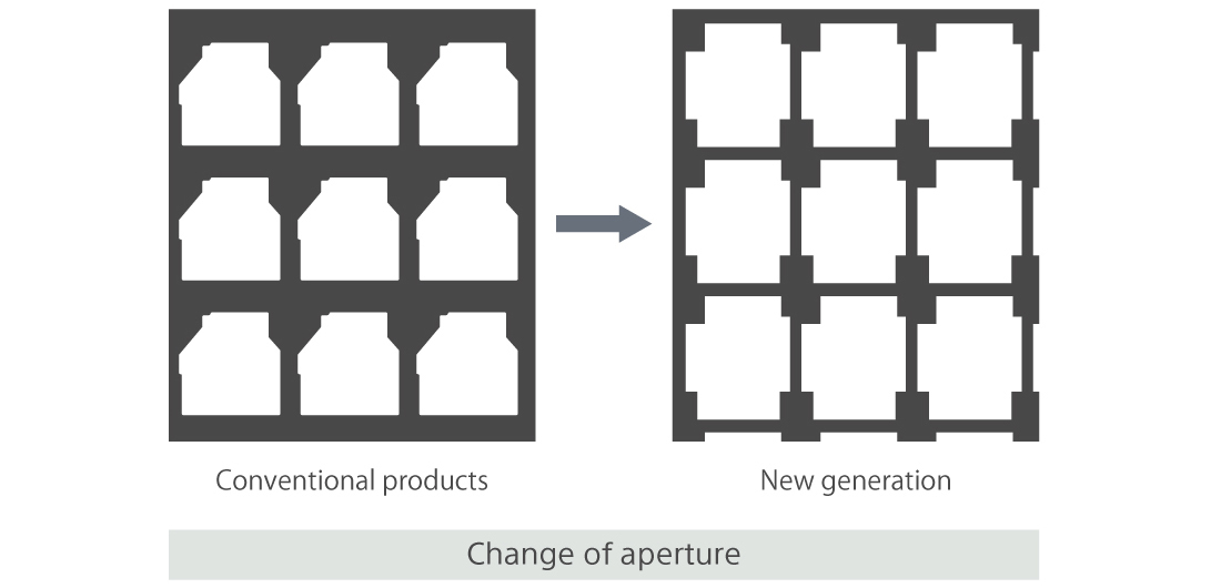
The transmissive type liquid crystal microdisplays have 2.3 million*1 pixels arranged vertically and horizontally and the transistors to turn those pixels ON/OFF are arranged for each pixel. In addition to this, there is also a lattice arrangement of metal wiring for the gate lines to transmit the ON/OFF signals for the transistors and the signal lines to transmit the pixel brightness signals (electric potentials). The transistors, gate lines and signal lines do not transmit light, so the areas excluding these parts are the aperture, which is the areas where the light passes through as the pixel. Therefore, in order to increase the transmittance of transmissive type liquid crystal microdisplays, it is necessary to make the transistors smaller and the metal wiring narrower.
SSS had already developed high-efficiency transmissive type microdisplays utilizing the fine fabrication technologies developed for image sensor processes. However, for the most recent generation of products, a contact plug has been adopted for the connection of each layer to realize more than a 20% increase in the numerical aperture*2 compared with the previous products.
*1) In the case of WUXGA.
*2) Proportion of the pixel area that is the aperture area.

High transparency double microlens technology<HTPS>
In addition to fine TFT technology for higher aperture ratios, another important technology to improve the light efficiency on transmissive type liquid crystal microdisplays is microlens technology. Microlenses are lenses that are installed for individual pixels to efficiently transmit the light from the pixel aperture, which is just several microns along one side. In addition to the microlenses on the light incidence side of the liquid crystal microdisplay, double microlens technology is to mount the microlens on the TFT substrate of the light emission side to maximize the microlens effectiveness. The microlens on the light incidence side focuses the light on the aperture of the pixel, and the microlens on the light emission side has the role of suppressing the spread of the transmitted light. The use of photolithography technology from semiconductor manufacturing makes it possible to produce aspherical profiles with high accuracy. With this technology, we succeeded in increasing the light efficiency on high resolution panels by 1.5 times*3.
*3) Compared with panel with no microlenses installed.

High light fastness TFT technology<HTPS>
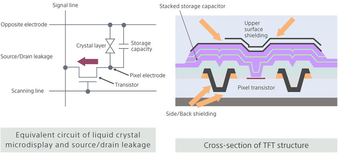
In general, liquid crystal displays display an image by transmitting the signal (electric potential) that determines the brightness to each pixel. The electric potential is maintained until the next electic potential is sent by both the capacity formed by the pixel electrode and counter electrode, and the holding capacitor as a buffer for each pixel. However, on a transmissive type liquid crystal microdisplay, the structure means that the light passes through close to the transistor, so there is an issue of photoconduction phenomenon that the light can lead to source-drain leakage on the transistors and change of the pixel electric potential can occur. Leaking of the pixel electirc potential can reduce the image quality, such as with screen flickering and roughness. The higher the luminance of a projector is, the greater the effects of light on the transistor characteristics will be, so high light fastness is required for higher luminance projectors. To achieve this, the most recent generation of products have a light shielding structure on the transistor surface, side faces and rear face, and also a stacked structure has been used in place of the previous planar structure, which has achieved compare to 70% increase in the storage capacity to hold electric potential from the conventional product.
Related Products & Solutions
-
Microdisplay
Liquid Crystal Microdisplay
Find out more about the liquid crystal microdisplay products using this technology.
Contact Us
For inquiries about Sony Semiconductor Solutions Group and products / solutions, specifications, quotation / purchase requests, etc., please contact us using the Inquiry form from the button below.