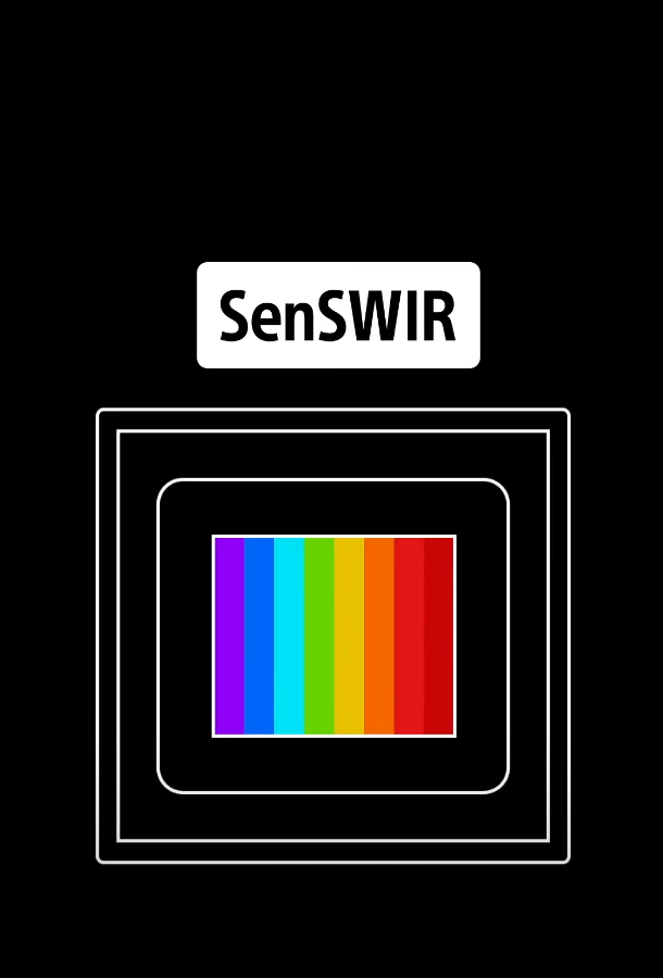
Small and high-resolution SWIR Image Sensor with the Industry’s smallest pixel size*1
will bring about innovation in the world of inspection.
October 27, 2021
SWIR (short-wavelength infrared) image sensors are pivotal in quality inspection across industries. The SWIR spectrum, a range of infrared spectrum outside the visible light band, can be used in product inspections to detect minute defects or contaminants that are invisible to the human eye. The SWIR image sensor we have developed only recently realizes a smaller size with more pixels by deploying the industry’s smallest*1 pixel of 5 µm. This image sensor is unparalleled as its dynamic range also covers the visible light spectrum. Behind this one-of-the-kind image sensor is a story of challenges that had no precedence in the development process. The story of how these challenges were overcome reveals the know-how only possessed by Sony Semiconductor Solutions Group (hereafter “the Group”). We explored the journey of the development of this SWIR image sensor that gives us a glimpse of the Group’s strengths in the development to create something totally new in the whole world.
*1:Among SWIR sensors employing a compound indium gallium arsenide (InGaAs) semiconductor, according to Sony' s research (as of May 2020).
M.Osawa
Sony Semiconductor Solutions Corporation
Imaging System Business Division
S.Maruyama
Sony Semiconductor Solutions Corporation
Research Div.1
K.Tsuji
Sony Semiconductor Solutions Corporation
Imaging System Business Division
T.Ogasawara
Sony Semiconductor Solutions Corporation
Imaging System Business Division
Sony’s first-ever SWIR image sensor
We already had all the technology that overpower competitors
―― What are SWIR and SWIR image sensor?
Maruyama:SWIR (short-wavelength infrared) is a particular range of infrared light. Some ranges of infrared light can be detected using a thermographic camera to measure temperatures, for example, of a human body. Others have different properties. And SWIR is a range of wavelengths between 0.9 and 2.5 µm.
It is characteristically different from visible light in terms of reflection and absorption, and the SWIR image sensor utilizes these characteristics to visualize what the human eye cannot perceive. Meanwhile, some materials allow SWIR light to penetrate through, which makes it possible to inspect what is behind these materials.
This light is also less scattering than visible light, and this characteristic is useful to visualize objects in a foggy or misty environment.
The SWIR image sensor we have developed can not only visualize within the range up to 1.7 µm, but also capture images in the visible light spectrum, thanks to our original technology.

―― What are the applications for SWIR image sensors in terms of industries and purposes?
Osawa:SWIR light has the properties to penetrate silicon and visualize moisture. Leveraging these properties, the image sensor finds applications in a variety of industries, including the semiconductor and food productions, mainly for inspection purposes. Take the semiconductor industry, for example, semiconductor wafers are normally made of silicon, which absorbs visible light. Using a conventional digital camera in visible light conditions it would simply look like a plain metal plate. Meanwhile, SWIR penetrates silicon. So, when visualized in an image captured by a camera equipped with SWIR image sensors, the wafer will look like a transparent glass pane, and cracks within the wafer or contaminants in the semiconductor can be detected.
Other than this, water is transparent under the natural visible light, but it absorbs a certain wavelength within the SWIR band, so it appears colored in a captured image. This characteristic can be utilized to detect moisture, thus the sensor can be used in food inspections, for example, to detect bruises and scratches in fruits, which are hard to detect under visible light.
Under visible light

Under SWIR imaging conditions

―― What difficulties did conventional SWIR image sensors have?
Osawa:SWIR image sensors have already been employed in many industries, but they had major technical issues. One of them was the pixel size. The pixels in conventional sensors are large, and the size makes it difficult to put many pixels in one sensor. It posed a challenge in raising the resolution. In terms of the image quality, too, there were difficulties in achieving clear images, so that camera manufacturers had to arrange heavy post-processing. In addition, because the sensors are an analog type, the camera had to convert the signals into digital data, which put a significant strain on the camera’s processing circuit and required design know-how to achieve it.
Maruyama:Conventional SWIR image sensors use bump connections, which involves metal balls to connect the indium phosphide layer with the silicon layer within the pixel. In order to reduce the pixel size using the bump connection, it is necessary to align the metal balls precisely at the bump pitch of micrometers, which in itself is very difficult to achieve. This technical difficulty has hindered upon the miniaturization of pixels, resulting in higher prices of image sensors.
―― How did you start the development of Sony’s first SWIR image sensor?
Maruyama:As I just mentioned, the miniaturization of SWIR image sensors had been hindered by the use of bump connection. We already knew that this problem could possibly be solved using the Cu-Cu connection*2, which is the stacking technology Sony had developed for years for image sensors. This technology would make it possible to align pixels at a micro-pitch. Meanwhile, conventional image sensors use silicon as a photoelectric conversion layer, but this material does not absorb the SWIR range of light. So, we needed to use indium gallium arsenide (InGaAs) as the photodiode material that can absorb the SWIR spectrum and convert the light energy into electric signals. This material was never used in Sony’s image sensors before, but however, Another division of Sony had the compound semiconductor technology to produce InGaAs. Furthermore, the Group had the technology for circuits to convert light energy into digital signals. The truth is that we already had necessary technology at hand to address the challenges, including the compound semiconductor technology required for the SWIR image sensor. We thought that it might be possible to realize a SWIR image sensor at an unprecedented miniature scale with an increased pixel count by combining these technologies. This led to the launch of our project team.
*2:Technology that provides electrical continuity via connected Cu (copper) pads when stacking the back-illuminated CMOS image sensor section (top chip) and logic circuits (bottom chip). Compared with through-silicon via (TSV) wiring, where the connection is achieved by penetrating electrodes around the circumference of the pixel area, this method gives more freedom in design, improves productivity, allows for a more compact size, and increases performance.
―― What were your main concepts for, and points to be realized in, the development?
Tsuji:We were already confident that the Group’s technical expertise would enable a success, so we focused on how to deploy the Group’s technology to make the resulting image sensor useful to clients. The first thing we did was to adopt the Column-Parallel A/D Conversion Circuit, a technique developed for CMOS image sensor technology, to digitize the SWIR image sensor output. This eliminated the need for camera manufacturers to provide A/D conversion components for post-processing. It also facilitated to resolve the image quality issues which our competitor products had to address. So, I believe that it helped to significantly reduce the image editing steps for camera manufacturers. In addition, we embedded a digital thermometer in the image sensor to make temperature control easy for cooling the device because InGaAs is very susceptible to temperature fluctuations.
Maruyama:We already knew that pixel miniaturization was possible to achieve, but we asked ourselves, should we as Sony be just content to achieve what we know we can do?
SWIR image sensors have photodiodes made of InGaAs. Indium phosphide (InP), which is indispensable for making InGaAs, forms a layer which blocks visible light. However, the Cu-Cu connection, which we considered adopting, structurally allowed to reduce the thickness of the InP layer. This led us to aim for developing a unique SWIR image sensor that was also able to capture images under visible light.

Osawa:The idea behind this decision was that, if it was realized, the sensor could be combined with multi-spectrum or hyper-spectrum systems to widen the wavelength coverage and to significantly enhance the image sensor’s market value.
Maruyama:Another point was that conventional SWIR image sensors had many defects. White patches would appear in the dark image due to the quality issues particular to InGaAs. We had the technology to make compound semiconductors based on our years of expertise in developing laser technology, so we aimed to leverage it in creating defect-free, high-quality products.
Ogasawara:I was responsible for the package specifications. I worked on the designing and implementation of the cooling system specifications for the ceramic PGA package with built-in thermoelectric cooling device (hereafter “the cooling package”).
Since SWIR is subtler than visible light in terms of light energy, and the image sensor that captures it is inevitably equally sensitive, it is very susceptible to temperature fluctuations.
It was important to cancel the effect of temperature in order to maximize the performance of the high image quality sensor.
So, I thought we would need to develop, in addition to a standard package, a package with a built-in cooling system.
This cooling system, however, cannot be simply cooling, for that would generate condensation. The solution was to make the sensor hermetic. Digitization within the sensor inevitably increases the number of terminals that come out of the package, which take up the available space for heat radiation inside the package. It was therefore important to ensure that the specifications had the right proportion between these two aspects.

While we were convinced of our chance of creating an image sensor that outplays competitors by far,
we had to face more than 300 challenges in the early stages of the development
―― What difficulties did you have to deal with during the development?
Tsuji:As it was the Group’s first-ever SWIR image sensor to be developed using InGaAs, we thoroughly reviewed challenges to be addressed, which resulted in more than 300 in the early stages of the development. As we proceeded further into the development, we found more issues to deal with. There turned out to be so many challenges awaiting. There were also phenomena unique to InGaAs, which were unknown with silicon, and we had to discuss how these might be handled in the end product.

Maruyama:We the image sensor development team had no expertise in InGaAs, but we knew that our neighbor, the laser development team, was well versed in compound semiconductors, and they could make InGaAs with this technology. So, we came to a conclusion that we should team up with them from the beginning to pursue the technological development.
It was also the first-time experience for the manufacturing to handle InGaAs, and for this reason we decided to invite members of the manufacturing to join us in the development stage in order to always proceed with the manufacturing process in mind. This was necessary. While silicon-based image sensors can be mass-produced on large wafers, InGaAs-based ones could previously be only realized on smaller wafers. This issue would necessarily give rise to challenges in terms of cost and supply capacity, and if failing to resolve these, the resulting product would not be market-worthy.
Ogasawara:Unlike the development of ordinary image sensors, this project involved many people, and the roles and team structure were different from usual ones. As a sub-product leader, I took great care to ensure appropriate information flows in order to enable each team to perform their given roles and collaborate with the others.
The severest difficulty we encountered in the package development was the failure of the cooling system in the production phase, despite that it worked well in the prototype. It would be a fatal error if a product with a cooling package could not deliver a cooling effect. We therefore went back to the drawing board to thoroughly review the design.

Osawa:The Group’s quality control is very strict. Though this was the first kind of SWIR image sensor for us, I think the development and manufacturing teams gave their best efforts to ensure the product quality as high as our CMOS image sensors.
―― What were the key breakthrough points for those challenges?
Tsuji:Normally, it is the project leader’s responsibility to take an initiative in managing issues and finding solutions. However, the numerous challenges, in fact over 300, were too many for one individual to handle. So, I distributed the challenges to relevant teams while I took up ones that concerned more than one team. Despite the number of challenges to be overcome, the prototype had positive feedback from our clients. We were very encouraged by their responses, such as “the image quality is exceptional,” which helped to hold high our team members’ morale, enabling us to follow through the development processes.
As for the phenomena that were unique to InGaAs, we made information readily accessible to the clients and ensured that they properly understood the characteristics of this sensor.
Maruyama:Regarding the issue of realizing larger wafers, we knew from the beginning that the only solution would be to cut and paste. But the problem was the pasting technique. There were some ideas, but none of them worked. I decided to speak to various engineers in the Group for their advice. It is my policy that everyone is on an equal standing where it comes to technological engineering. So, I spoke literally to everyone, from seasoned engineers to fresh faces. I had so many different ideas from them, and considered and tested them until I found a breakthrough point. Some of the ideas were unrelated to semiconductors. These were ones we could not have come up with ourselves. In fact, the enlargement of wafer was made possible based on such ideas.
We have an excellent diversity in the Group, and members are always willing to offer ideas. The workplace culture allows us to be approachable, and we do not hesitate to help. Some even go further to join the team voluntarily. They willingly offer their helping hand to show us what they mean if explaining their ideas on a whiteboard would not get us enlightened. This is how engineers are: they get more excited as the challenge poses greater technical difficulties.

Ogasawara:For me, there is a person in the Group who knows heat very well. I would want to ask him for his opinions, but before doing this, I would need to clarify where exactly this problem about heat may come from because this person I would like to consult is not an expert in image sensors. Unless I have a good idea about what I want to ask, he may find it difficult to answer. So, even if my knowledge about heat is insufficient, I need at least to identify facts and have a good sense of whereabout the problem lies. That is exactly what I did.
I went back to square one and tried to understand how heat was transmitted. Then I ran a simulation, used a test piece to measure the heat transmission, scrutinized the heat movements in this package, and finally identified the cause that prevented the cooling effect from happening. As a result, I learned based on this understanding what kind of evaluation was required for quality control in the process of moving toward the final product.
The sensational Sony’s SWIR image sensor
will bolster the potentials in the market
―― What solutions can be expected from Sony’s SWIR image sensors?
Osawa:The increased pixel count through pixel miniaturization brings about immense benefits. The image sensor enables to discern infinitesimal damage that could not be detected before, improving the inspection quality. The digitization will make camera design easier, which would in turn help to economize on cost, etc. and make the image sensor more affordable for clients. As we believe in the work to bring better quality inspection to the world, we are convinced that this SWIR image sensor will play a significant role in it. Also, we already have excellent client feedback.
Our SWIR image sensor has the Group’s acclaimed characteristics, such as the ease of use, high performance, and many more. I believe that it will cause a sensation in the market. I think that those characteristics will help to pave a way toward new applications, too.
―― What are the future prospects for SWIR image sensors?
Osawa:Generally speaking, AI is considered to facilitate improvements in the inspection accuracy with image sensor. But for this to be the case, it is important that AI learn from high quality images. If, I think, AI is fed with high-definition images captured using our image sensors, it may possibly improve the accuracy of the sensors so that they become able to find events so minute that they could not have detected before. Also, they just may be able to elevate inspection quality to a new, unprecedented plain if the sensors realize a hyper-spectrum inspection, covering the visible light and SWIR bands.
―― What would be your next challenges?
Osawa:This Sony’s first-ever SWIR image sensor is a product of the passion of so many people who were involved in its development. I would like to promote this SWIR image sensor to such clients who have been unable to afford to—and those who have not even considered—introducing it, to positively consider this as an option. There are numerous possibilities in the SWIR spectrum, and I believe that a diversity of clients can benefit from them to satisfy their needs. I would do my best to support as many clients as possible to identify their challenges and find solutions.
Tsuji:I would like to make this SWIR image sensor widely accessible, even to the clients who have never used this type of image sensor. To this end, there is still much room for improvement to make it easier to use. I hope it will become as easy for anyone to use as our CMOS image sensors of the Group.
Maruyama:I think that this SWIR image sensor could also be improved more in terms of performance. Though I am confident that it already is many steps ahead of its competitors, I will continue my efforts to ensure its absolute winning position in the future. I will be striving toward our own one-of-the-kind sensors with various, original features which only we can realize.
Ogasawara:The development has given us many experiences that were new to us. Once the product is out in the market, we will be hearing various responses from our clients. I would very much appreciate such feedback and make it a stepping stone for even better products. As for the package, I think it will take much more thinking and analyzing in order to make the next step for a better, easier-to-use product. I will be dedicated to the next, better adapted package for the future product that will surpass customer expectations as we work on client feedback.
※This button will redirect you to the salesforce.com Co., Ltd. website, which we have entrusted.